• Home
  • Faq’s
  • About Us
  • Contact Us

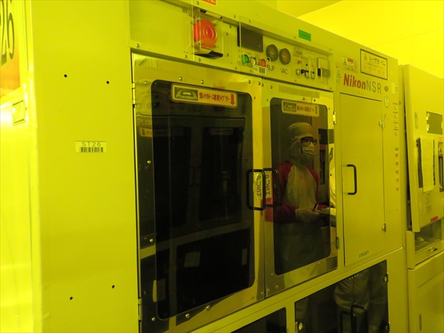
NIKON i7aNSR-1755i7

NIKON i7aNSR-1755i7

Call for a Quote

Categories ,

Description

The Nikon NSR-1755i7A is an i-line wafer stepper used for high-throughput, mature semiconductor manufacturing, featuring a 0.55µm resolution and supporting wafers up to 200mm. It is commonly used for MEMS, power devices, and analog IC production, often utilizing a three-zone illumination source to optimize throughput and stability.

CAEOnline +4
Key Features and Specifications
  • Resolution & Accuracy: The system provides a resolution of
  • 0.55
  • 𝜇𝑚

    (on 8-inch wafers) and a depth of focus of

  • <0.6
  • 𝜇𝑚

    .

  • Throughput & Performance: It offers high-speed scanning (up to 800 mm/s) and uses a three-zone illumination source to boost efficiency.
  • Compatibility: Supports varied substrate sizes, including 50mm, 100mm, 150mm, and 200mm wafers.
  • Advanced Controls: Includes a programmable aberration corrector for improved image quality and a CCD-based automated alignment system.